 русский
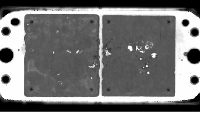
Core Applications of Scanning Acoustic Microscopy (SAT) in IGBT Testing
Date:2026-05-09Views:0
The application of Scanning Acoustic Microscopy (SAT) in the Insulated Gate Bipolar Transistor (IGBT) domain is crucial, playing a pivotal role in ensuring the reliability and integrity of high-power electronic modules.
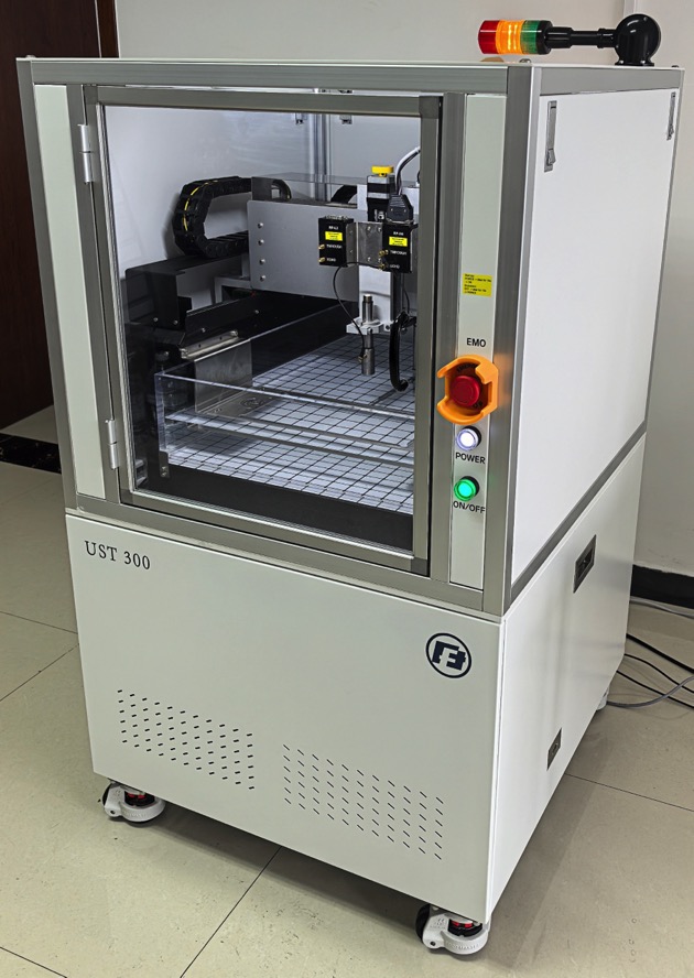
I. Core Detection Capabilities
A. Critical Defect Identification
- Delamination and Pseudo-solder Defect Detection: By utilizing high-frequency ultrasound (e.g., 50 MHz}), SAM penetrates the multi-layer structure of IGBT modules. It accurately identifies defects such as delamination, voids, and empty solder joints at the interfaces between the chip, ceramic substrate, and copper layers. The sensitivity to these flaws significantly surpasses that of X-ray inspection.
- Micro-crack and Foreign Material Detection: The technique can detect micro-scale cracks in welding joints and foreign inclusions within the material, supporting cross-sectional tomography (up to 50 layers) to precisely localize defect positions.
B. Non-Destructive Full-Dimensional Analysis
- Assessment Method: Without damaging the $\text{IGBT}$ module structure, SAM generates 2D/3D images based on ultrasonic reflection signals.
- Output Data: It visualizes defect area, depth, and distribution, making it perfectly suited for large-scale, full-module inspection.
II. Technical Advantages and Innovations
A. High-Resolution Imaging
- Capability: High-frequency probes (e.g., $50\text{ MHz}$) deliver micron-level resolution, allowing clear visualization of minute voids (potentially nanoscale) and the exact boundaries of delamination.
B. Smart Automated Inspection
- System Integration: Seamless integration with Manufacturing Execution Systems ($\text{MES}$) allows for automated data upload and statistics.
- Process Improvement: Supports automatic defect area calculation and report generation. Furthermore, smart algorithms classify defect types (e.g., void vs. crack), minimizing human misjudgment.
C. Multi-Scenario Adaptability
- Versatility: The technique is adaptable to inspecting complex structures, including liquid-cooled heat sinks, ceramic substrates, and automotive IGBT modules, meeting the demanding requirements of high-end sectors like New Energy Vehicles and Photovoltaic Inverters.
III. Typical Application Scenarios
- New Energy Vehicle (NEV) IGBT Module QC:
- Inspection of critical components like On-Board Chargers ($\text{OBC}$) and motor controllers to prevent thermal runaway risks caused by pseudo-solder joints or delamination.
- Process Optimization and Reliability Verification:
- Optimizing welding parameters (e.g., temperature, pressure) by analyzing delamination defect data to improve the $\text{IGBT}$ module yield.
- Comprehensive life-cycle reliability screening for IGBT modules in sectors like aerospace and rail transport.
IV. Comparison with Traditional Inspection Methods
| Detection Method | Advantage | Limitation |
|---|---|---|
| SAM (USM) | Non-destructive, high resolution, supports multi-layer tomography. | Requires coupling medium (e.g., immersion in water). |
| X-ray Inspection | Penetrates dense structures. | Low sensitivity to air-filled defects; involves radiation risk. |
| Destructive Testing | Direct observation of physical performance. | High cost, cannot perform full inspection, sample waste. |
Conclusion: Owing to its non-destructive nature, high precision, and smart automation capabilities, SAM has become an indispensable inspection tool in $\text{IGBT}$ manufacturing and reliability validation. It is driving the power electronics industry toward higher reliability and greater miniaturization.
Related News